




We went looking for the Sohu spec sheet, and it is not there any more. Etched raised 300 million dollars on July 23 at a 10.3 billion dollar valuation, led by Sequoia with a16z, Jane Street, Diffusion and SK hynix, roughly double the 5 billion it was worth in December. Then here's the part nobody seems to have flagged: search etched.com for the word transformer and you get zero hits. Same for Sohu. The company that made its name in June 2024 selling the first chip built to run only one neural network architecture now sells Frontier Inference Clusters, aimed at trillion-parameter sparse MoEs and long context. That isn't a rebrand. It's a different bet, and probably a smarter one. It also means the 20x an H100 figure still circulating describes a product Etched has stopped describing.
The short answer
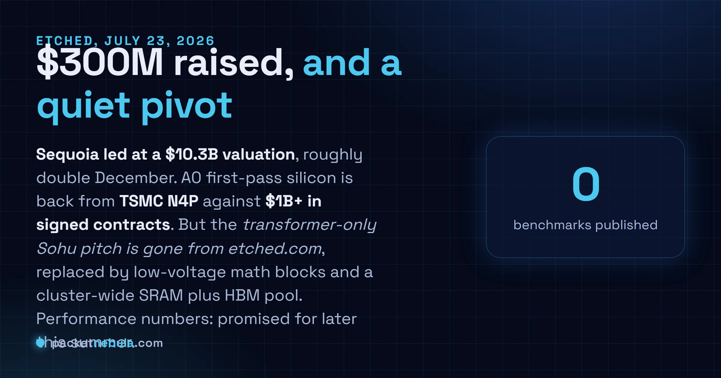
Etched raised 300 million dollars led by Sequoia, doubling its December mark. The interesting part is not the money. The transformer-only ASIC pitch that made the company famous is gone from its own materials, replaced by two architecture claims: math blocks at under half the usual voltage, and a shared SRAM plus HBM pool across the cluster. A0 silicon on TSMC N4P is real. Performance numbers are promised for later this summer. Nothing here is buyable today.
What actually got announced
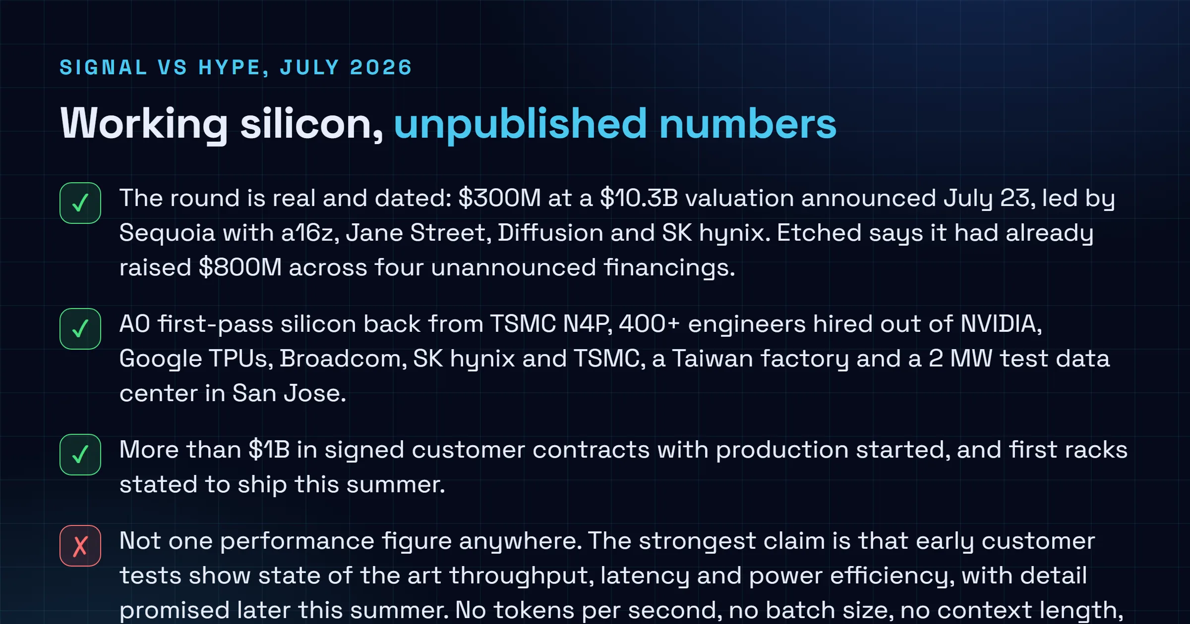
The round is straightforward. 300 million dollars, 10.3 billion valuation, Sequoia leading, with a16z, Jane Street, Diffusion and SK hynix in. Sequoia’s Sonya Huang framed it as a bet that “inference is on the path to becoming the largest market in the world, and purpose-built compute will power the majority”. Gavin Uberti, the CEO and one of three Harvard dropouts who started the company in 2022, was blunter: “Now is the time to be aggressive. Our chips work, people want them, and it’s time to ship.”
The operational details are the ones we’d actually weigh. 400-plus engineers, hired out of NVIDIA, Google TPUs, Broadcom, SK hynix and TSMC. A0 silicon, meaning first-pass working parts, back from TSMC on N4P. More than a billion dollars in signed customer contracts with production started. A Taiwan factory, a test house and prototyping lab plus a 2 MW data center at the San Jose office, and per TechCrunch a new 80,000 square foot site in Milpitas with 10 MW.
That is a real company building real hardware. Which is worth saying plainly, because for two years the standard take on Etched was that it was a pitch deck with a wafer photo.
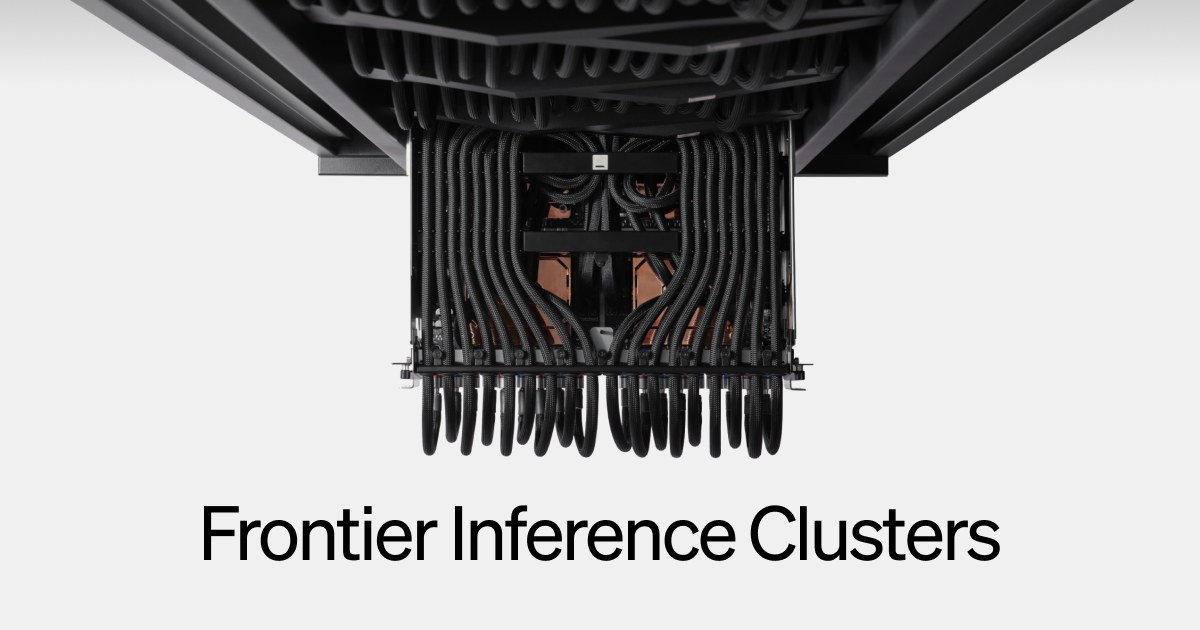 Image: Etched (company announcement image)
Look at the caption Etched chose for its own announcement image. Frontier Inference Clusters. Not a chip name.
The word that disappeared
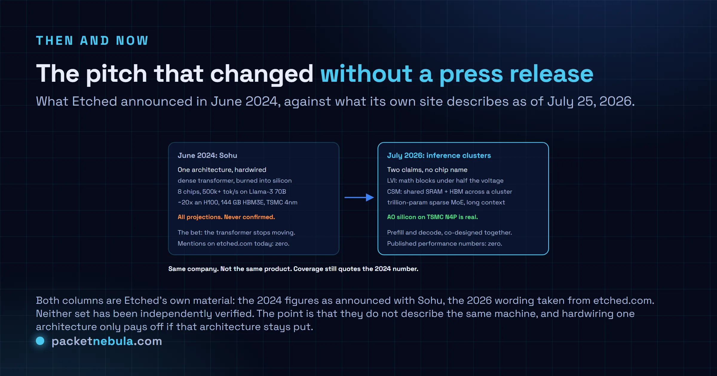
June 25, 2024. Etched announced Sohu and got the whole industry arguing for a week. The pitch was absolutist: the first commercially marketed chip designed to run one neural network architecture and nothing else, the transformer, hardwired into silicon. Eight chips in a server, more than 500,000 tokens per second on Llama-3 70B, roughly 20 times an H100, 144 GB of HBM3E, TSMC 4 nm. Every one of those numbers was a projection, and none was ever independently confirmed.
Now grep the company’s site. Transformer: zero. Sohu: zero. What’s there instead is a paragraph saying the systems are “built to push the entire pareto curve on frontier models, including many-trillion-parameter MoEs, long context, and agentic workloads”, covering “both prefill and decode”.
Read those two pitches back to back and it’s a different company. Hardwiring one architecture is a bet that the architecture stops moving. Between June 2024 and now the workload went sparse, context went long, and agent loops turned inference into a latency problem rather than a throughput problem. A chip that froze a 2024 dense transformer dataflow into silicon would be arriving into a market it was shaped wrong for.
So I read the pivot as the good news, not the scandal. They looked at where inference went and rebuilt around it. What bothers me slightly is that nobody in the coverage said so. Half the write-ups this week still lead with the 20x H100 line, which now belongs to a design the company itself has stopped naming.
LVI is the claim worth understanding
Two named breakthroughs, and one of them is genuinely interesting.
Low Voltage Inference is the pitch that AI chips can’t scale FLOPs without thermal throttling, because utilisation drives power up and the clock gets pulled down, leaving sustained throughput “under half of Peak FLOPs”. Etched says it runs its math blocks at under half the voltage of most AI chips, buys “multiple times the FLOPs density” with that, and holds above 80 percent of peak FLOPs on trillion-parameter sparse MoEs without throttling.
Why that isn’t nonsense: dynamic power goes as capacitance times voltage squared times frequency. Halve the voltage and, in the ideal case, you’re at about a quarter of the dynamic power for the same clock. That’s not a trick, it’s the reason undervolting works on your own GPU. The catch is that everything gets harder down there. Timing margin shrinks, SRAM has a minimum operating voltage of its own, and device variability across a big die stops being a rounding error. Etched’s own list of what LVI required (splittable math arrays, new tiling and scheduling, power delivery networks, VRM architecture, packaging, cold plates) reads like an honest account of that difficulty.
Cluster Scale Memory is the second half: a hybrid SRAM and HBM design with a shared low-latency pool across the whole scale-up domain, over a proprietary interconnect. The argument is that HBM-only parts can’t hit SRAM-speed decode while SRAM-only parts give up capacity and FLOPs density, so you want both. SK hynix sitting on the cap table reads as a supply signal for exactly that.
Here’s what’s missing from all of it. Not one number. The strongest performance statement anywhere in the announcement is that “early customer tests show us achieving SOTA throughput, latency, and power efficiency on inference workloads”, followed by a promise to share performance and roadmap detail “this summer”. No tokens per second, no batch size, no context length, no cost per million tokens, no MLPerf entry. Compare that to the AMD launch two days earlier, where we could at least audit the footnotes under the claims and re-do the arithmetic. Here there’s nothing to audit.
Everyone split prefill from decode this week
Etched saying “both prefill and decode” lands in a strange week for that phrase. On the same day, July 23, AMD and Cerebras announced a disaggregated inference system that does exactly the split: AMD Helios racks as the throughput engine, Cerebras wafer-scale parts doing low-latency decode and token generation, claimed at up to 5x tokens per second per watt, arriving first on Cerebras Cloud in the second half of 2026.
Two teams, same diagnosis. Prefill wants raw FLOPs, decode wants memory latency, and one uniform pile of GPUs is a compromise on both. AMD and Cerebras solve it by bolting two different machines together. Etched claims to solve it inside one co-designed cluster. Nobody has published numbers for either approach yet, so pick your prior, but the architectural direction is no longer in dispute. Custom inference silicon is the live question of this cycle, which is also why OpenAI is building its own.
What we’d watch
Nothing to do this week. You cannot buy, rent or benchmark an Etched rack, and no public price exists.
When the promised summer update lands, four things tell you whether it’s real. Does it name a model, a batch size and a context length, or is it another “SOTA” with no axis labels. Does it quote cost per million tokens, since power efficiency claims that never turn into a price are marketing. Does any party outside Etched get a rack and say something. And do the billion dollars of contracts convert into named customers, because signed and shipped are different verbs, and the site’s own line is that it’s still “validating our first rack-scale product with customers”.
One honest counterweight to my own skepticism: A0 first-pass silicon on a leading node is genuinely hard, and a team of 400 ex-NVIDIA and ex-TPU engineers plus a memory vendor on the cap table is not a vibe. I might be wrong to want the numbers first. I’d still rather have them.
Sources
Primary: etched.com (checked July 25, 2026, for the Low Voltage Inference and Cluster Scale Memory descriptions, the A0 and TSMC N4P claim, and the absence of any Sohu or transformer mention) and the funding announcement on GlobeNewswire. Coverage and context: TechCrunch and Blocks & Files. On the original 2024 Sohu claims: TechPowerUp. On the AMD and Cerebras split: AMD Newsroom.
Frequently asked questions
How much did Etched raise, and at what valuation?
300 million dollars at a 10.3 billion dollar valuation, announced July 23, 2026. Sequoia led, with a16z, Jane Street, Diffusion and SK hynix participating. Etched says on its own site that it had previously raised 800 million dollars across four unannounced financings, so total funding is now north of 1.1 billion. TechCrunch reports the prior mark was 5 billion in December, which makes this roughly a doubling in seven months.
Is Etched still building the Sohu transformer-only chip?
Not under that name, and not under that pitch. The word Sohu does not appear anywhere on etched.com as of July 25, 2026, and neither does the word transformer. What the company describes instead is two things: Low Voltage Inference, running math blocks at under half the voltage of most AI chips, and Cluster Scale Memory, a hybrid SRAM and HBM pool shared across a whole scale-up domain. The stated target workloads are many-trillion-parameter MoEs, long context and agentic traffic, covering both prefill and decode. The 2024 Sohu pitch was the opposite shape: one dense architecture hardwired into silicon.
Has any of the performance been independently verified?
No. Etched claims A0 first-pass silicon success on TSMC N4P, says early customer tests show state of the art throughput, latency and power efficiency, and promises more detail on performance and roadmap later this summer. As of July 25 there is no published tokens-per-second figure, no per-token cost, no named batch size or context length, and no MLPerf submission. The 10.3 billion valuation currently rests on working silicon plus more than 1 billion dollars in signed contracts, not on a benchmark you can re-run.
What is Low Voltage Inference, in plain terms?
Dynamic power in a chip scales with capacitance times voltage squared times frequency. Drop the supply voltage of the math arrays and the power falls with the square of it, so in the ideal case running at under half the voltage buys you close to a quarter of the dynamic power at the same clock. Etched spends that headroom on more math per watt, and claims it can hold above 80 percent of peak FLOPs on trillion-parameter sparse MoE work without thermal throttling. The physics is textbook. The hard part is timing margin, SRAM minimum operating voltage and device variability at low voltage, which is engineering nobody can grade from a press release.
Can I buy or rent one today?
No. Etched says its first racks ship this summer against existing customer contracts, and that it is validating its first rack-scale product with customers now. There is no public price, no cloud you can sign up for, and no general availability date. If you are planning inference capacity for this year, this changes nothing in your budget yet.