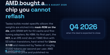





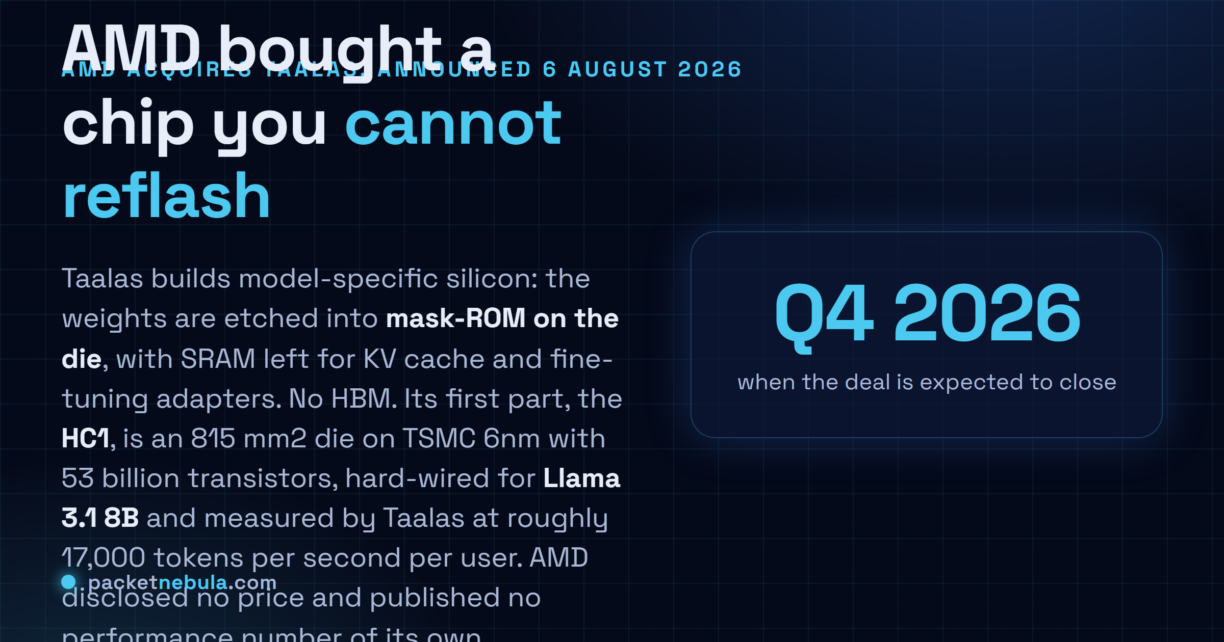
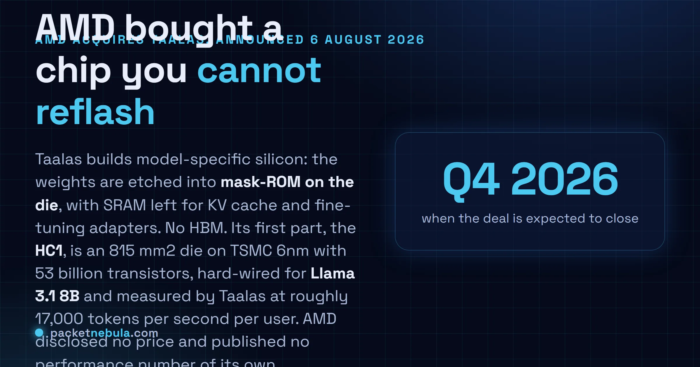
Picture a chip you can't reflash. That's the bet AMD just bought. On 6 August it signed a definitive agreement to acquire Taalas, a three-year-old Toronto outfit that etches model weights straight into the metal layers of a die instead of streaming them out of HBM. Terms weren't disclosed. Closing is expected in Q4 2026, pending regulators. Taalas' first part, the HC1, is an 815 square millimetre die on TSMC 6nm carrying 53 billion transistors, hard-wired for Meta's Llama 3.1 8B, and the company clocked it at roughly 17,000 tokens per second per user. Its own measurement, worth remembering. AMD says the technology joins its accelerator roadmap alongside Instinct, EPYC, Helios and ROCm, and published no performance figure of its own.
The short answer
AMD is buying Taalas, which builds chips with the model weights etched into mask-ROM instead of sitting in HBM. The HC1 is hard-wired for Llama 3.1 8B and Taalas measured it at about 17,000 tokens per second per user. Terms are undisclosed. AMD named no product, no price and no benchmark, and says the technology feeds the Instinct and ROCm roadmap. The catch is structural: a chip built around one model needs new silicon when that model moves.
What AMD actually agreed to buy
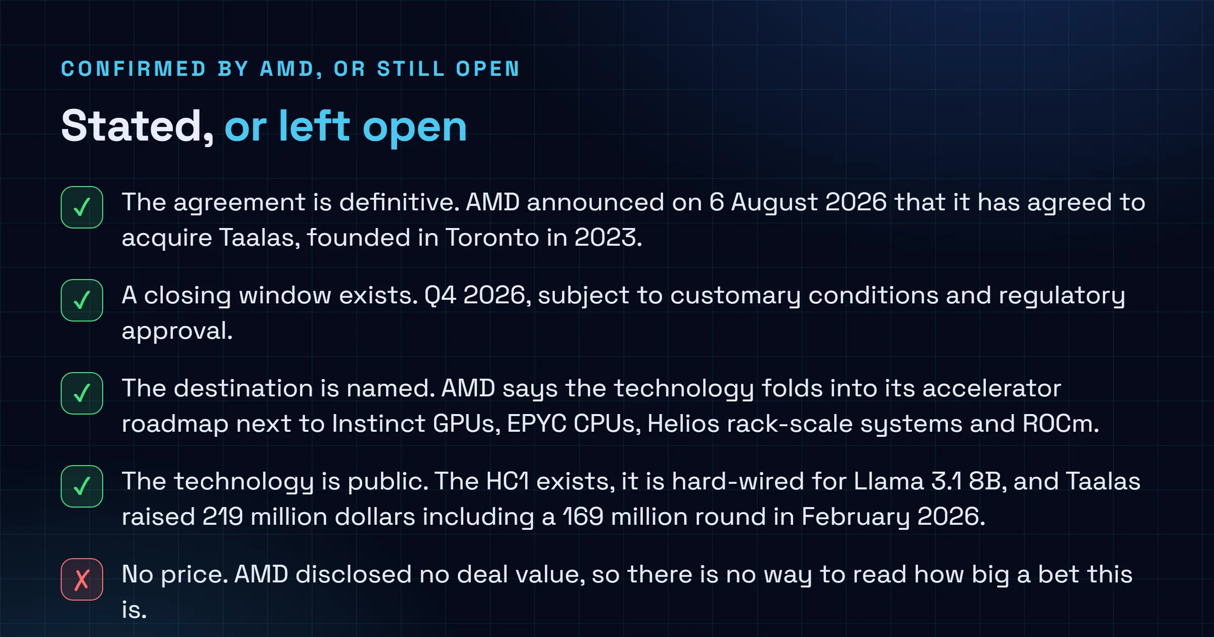
Taalas is small and specific. Founded in 2023 in Toronto by Ljubisa Bajic, Drago Ignjatovic and Lejla Bajic, it raised $219 million in total, including a $169 million round in February 2026 backed by Quiet Capital, Fidelity and the veteran semiconductor investor Pierre Lamond. Bajic’s history matters here: he was an architect at both AMD and Nvidia before co-founding Tenstorrent, so AMD is partly buying back a person it once employed.
The press release is thin in the way these things usually are. Vamsi Boppana, an AMD senior vice president, said the team and technology strengthen the AI portfolio by delivering differentiated inference performance and efficiency. No number attached. No product name. The one concrete commitment is that the technology gets integrated into the accelerator roadmap and into system-level designs with Instinct GPUs, EPYC, Helios rack-scale and ROCm.
So the announcement itself tells you almost nothing. The interesting part is what Taalas already published.
The trick is in the mask layers
Every conventional accelerator spends an enormous share of its power budget moving weights. The compute die sits next to HBM stacks, and for each token generated the weights get pulled across that link. It’s why memory bandwidth, not FLOPS, is the number people quote when they size inference hardware.
Taalas deletes that link. The weights are patterned into mask-ROM on the die during fabrication, in what the company calls a recall fabric, and a separate SRAM fabric holds the parts that genuinely change while the model runs: the KV cache, plus fine-tuning adapters. Nothing streams. The company’s marketing calls the result a Hardcore Model and claims 1000x the efficiency of the software equivalent, which is the kind of round number that should make you check the footnotes.
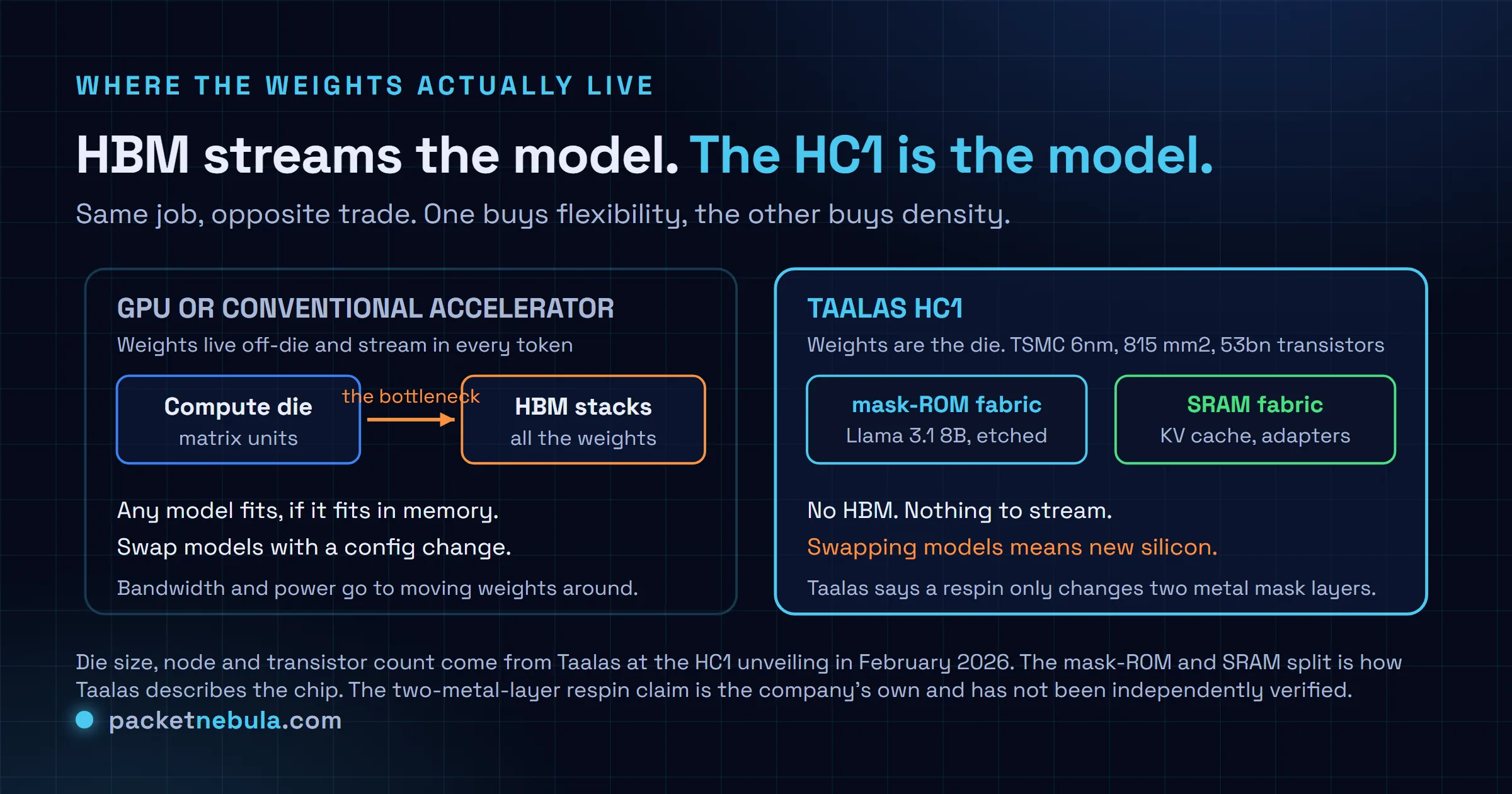
The HC1 is the proof point. TSMC 6nm, 815 square millimetres, 53 billion transistors, all of it arranged around one 8-billion-parameter model. Taalas measured it at roughly 16,960 tokens per second per user on Llama 3.1 8B, and when it announced the part in February it framed that as 48 times faster than Nvidia GPUs and 8.5 times faster than Cerebras accelerators. Those are Taalas’ comparisons, run by Taalas, and no independent lab has published a competing set. I’d hold them loosely. The architecture is plausible enough that a large gap wouldn’t surprise me, but “large gap” and “48x” are not the same claim.
Where this breaks
Here’s the part everyone glosses over. A chip built around a specific model is obsolete the day that model is superseded, and models are currently superseded roughly every quarter.
Taalas’ answer is that a new variant only touches two metal mask layers, not the whole stack, so a respin is cheaper and quicker than a fresh design. Fair. That’s a real engineering argument and it’s the reason the company exists rather than being an obvious non-starter. But cheaper than a tape-out is still a manufacturing run, a lead time and a physical swap in a rack. You don’t push it with a deployment.
The size ceiling is the other constraint. The HC1 carries 8 billion parameters on a die that’s already near the reticle limit. The second-generation HC2 targets 20 billion, with pipeline parallelism across several accelerators for anything bigger. Twenty billion is a useful size, it covers a lot of production classification and routing work, but it is not where the frontier lives. Which means this technology gets deployed by whoever runs one model, at enormous volume, for a long time. That’s a short list. Hyperscalers, a handful of model labs, maybe an inference provider with a stable flagship.
Does it change anything for you
Not this year. The deal hasn’t closed, AMD hasn’t named a part, and there’s no price.
What it does tell you is where AMD thinks the money is. Its current fight is at the top of the stack, where the MI455X and Helios line goes up against Vera Rubin on general-purpose training and inference. Buying Taalas is a bet on a different axis entirely: that a meaningful slice of inference will settle onto models stable enough to bake into a mask set. If that’s right, hard-wired parts undercut GPUs badly on cost per token for that slice. If it’s wrong, AMD spent an undisclosed sum on a very fast Llama 3.1 8B machine.
The pattern is familiar by now. OpenAI put its name on the Broadcom-built Jalapeno inference chip, and Anthropic confirmed a custom silicon team with no chip and no timeline. Everyone with a serious inference bill is trying to get off the merchant GPU curve. What separates the attempts is how far along they are, and Taalas is unusual in that the silicon already exists and already ran a real model.
Honestly, the thing I’d watch isn’t AMD’s roadmap slide. It’s whether any lab publicly commits to freezing a model long enough to justify a mask set. That commitment is the actual product here, and nobody has made it yet.
Sources
- AMD investor relations, “AMD Acquires Taalas to Advance Compute Solutions for Rapidly Growing AI Inference Market”, 6 August 2026, for the definitive agreement, the undisclosed terms, the Boppana quote and the Instinct, EPYC, Helios and ROCm integration plan.
- The Register, 6 August 2026, for the mask-ROM and SRAM recall fabric split, the 16,960 tokens per second measurement, the 48x and 8.5x comparisons, the two-metal-layer respin, the HC2 20 billion parameter target and the Q4 2026 closing window.
- ServeTheHome, for the HC1 die size of 815 square millimetres, the 53 billion transistor count, the TSMC 6nm node and the note that the comparison figures are Taalas’ own.
- Electronics Weekly, February 2026, for the $169 million round and the $219 million total, with Quiet Capital, Fidelity and Pierre Lamond named.
- Taalas, for the Hardcore Models framing and the 1000x efficiency claim, checked 8 August 2026.
Frequently asked questions
What exactly did AMD announce on 6 August 2026?
A definitive agreement to acquire Taalas, a Toronto company founded in 2023 that designs model-specific inference silicon. Financial terms were not disclosed. AMD said the deal is subject to customary closing conditions and regulatory approval, with closing expected in the fourth quarter of 2026, and that it intends to fold the technology into its accelerator roadmap alongside Instinct GPUs, EPYC CPUs, Helios rack-scale systems and ROCm.
What does it mean to etch a model into silicon?
Taalas splits its die into two regions. A mask-ROM recall fabric holds the model weights, physically patterned into the chip during manufacturing, and an SRAM recall fabric holds the things that do change at runtime: the KV cache and fine-tuning adapters. There is no HBM. The weights are not loaded, because they are the chip. That removes the memory traffic a GPU spends most of its power on, and removes the ability to run a different model.
Is the 17,000 tokens per second figure verified?
No. It is Taalas' own measurement of the HC1 running Llama 3.1 8B, published when the chip was unveiled in February 2026, and the same goes for the comparisons it drew against Nvidia and Cerebras parts at the time. AMD published no throughput number in its acquisition announcement. Nobody outside the company has run the part on a public benchmark, so treat every figure here as vendor-reported.
What happens when the model gets updated?
You need new silicon. That is the whole trade. Taalas softens it by saying a new model variant only requires changing two metal mask layers rather than a full redesign, which is genuinely cheaper and faster than a fresh tape-out, but it is still a manufacturing run and a hardware swap rather than a config change. This is why the approach fits stable, high-volume serving and fits nothing else.
Should this change what I build on today?
No. There is no AMD product, no price and no date, and the deal has not closed. The second-generation HC2, targeting 20 billion parameters, is still a plan. If you serve inference at scale, the thing worth watching is whether AMD names a model it intends to hard-wire, because that would tell you it believes some weights have stopped moving.